- Astronomy
- Biomedical Optics & Medical Imaging
- Defense & Security
- Electronic Imaging & Signal Processing
- Illumination & Displays
- Lasers & Sources
- Micro/Nano Lithography
- Nanotechnology
- Optical Design & Engineering
- Optoelectronics & Communications
- Remote Sensing
- Sensing & Measurement
- Solar & Alternative Energy
- Sign up for Newsroom E-Alerts
- Information for:
Advertisers
|
 |
|
|
Nanotechnology
High-quality single-crystal diamond nanophotonic and nanomechanical resonators
Behzad Khanaliloo, Matthew Mitchell, Aaron C. Hryciw, Harishankar Jayakumar, David P. Lake, Hamidreza Kaviani, John P. Hadden and Paul Barclay
A purely chemical quasi-isotropic diamond etch is used to undercut devices patterned from bulk diamond chips.
17 February 2016, SPIE Newsroom. DOI: 10.1117/2.1201601.006303
 In the discipline of cavity optomechanics, the interactions between photons and phonons are studied within a mesoscopic device geometry.1 Cavity optomechanical devices can be used to enhance optical forces and have paved the way for demonstrations of optically controlled mechanical vibrations. Diamond is an attractive material platform for such cavity optomechanical devices because of its large transparency window (from 220nm to far-IR wavelengths), large Young's modulus, high thermal conductivity, and low intrinsic dissipation.2 Diamond is also an attractive platform for studying spin-photon-phonon interactions using color centers, such as the nitrogen vacancy (NV).
 Recently, piezoelectrically actuated nanomechanical resonators have been used to manipulate the electron spins of diamond NV centers.3 This process enables coherent phonon–spin coupling for sensing4 and spin-mediated mechanical normal-mode cooling5, 6 applications. Realization of optomechanical structures from bulk single-crystal diamond can provide access to all-optical control of mechanical vibrations. If such structures can be achieved, it would be possible to replace previously required piezoelectric drives with integrated on-chip optical control. Recently, piezoelectrically actuated nanomechanical resonators have been used to manipulate the electron spins of diamond NV centers.3 This process enables coherent phonon–spin coupling for sensing4 and spin-mediated mechanical normal-mode cooling5, 6 applications. Realization of optomechanical structures from bulk single-crystal diamond can provide access to all-optical control of mechanical vibrations. If such structures can be achieved, it would be possible to replace previously required piezoelectric drives with integrated on-chip optical control.
In this study,7 we demonstrate high-quality mechanical resonators and optical cavities fabricated from single-crystal diamond. This work is thus a step toward realizing hybrid optomechanical-spin devices in diamond. Fabricating free-standing devices from single-crystal diamond, however, is challenging. This is because the material is not readily available in heteroepitaxially grown thin-film form. To overcome this hurdle, we developed a new fabrication technique (see Figure 1) to create optical and mechanical devices from commercially available single-crystal bulk diamond.8, 9 In the key fabrication step—see Figure 1(v)—patterns that have been transferred from a mask layer to a diamond substrate are undercut in a quasi-isotropic manner, using an oxygen (O2) plasma. No external bias is applied during this step, so that the O2 ions exhibit a random motion and thus provide a purely chemical etch environment. As a result, the etch windows are defined by the crystal planes of the diamond, as illustrated in Figure 2(a). Our fabrication technique is scalable, provides low levels of damage to the unetched areas, and can be easily implemented on standard nanofabrication tools.
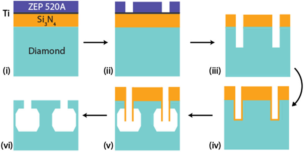
Figure 1. Schematic process flow for the fabrication technique used to create free-standing devices from single-crystal diamond, adapted from original figures. 8,9 (i) Sample is cleaned in piranha, and coated with silicon nitride (Si 3N 4) as a hard mask and ZEP 520A (an electron beam lithography, EBL, resist). A thin layer of titanium (Ti) is used as an anti-charging layer for EBL. (ii) Patterning is achieved using standard EBL techniques. (iii) Patterns are transferred to the hard mask and diamond substrate through inductively coupled reactive ion etching with octafluorocyclobutane–sulfur hexafluoride (C 4F 8-SF 6) and oxygen (O 2) etch chemistries, respectively. (iv) An additional Si 3N 4 mask is used to protect the diamond sidewalls during the plasma undercut. (v) A purely chemical quasi-isotropic diamond etch is used (with O 2 and zero bias) to undercut the patterned devices. (vi) Si 3N 4 is removed using hydrofluoric acid and is cleaned in a boiling piranha solution.
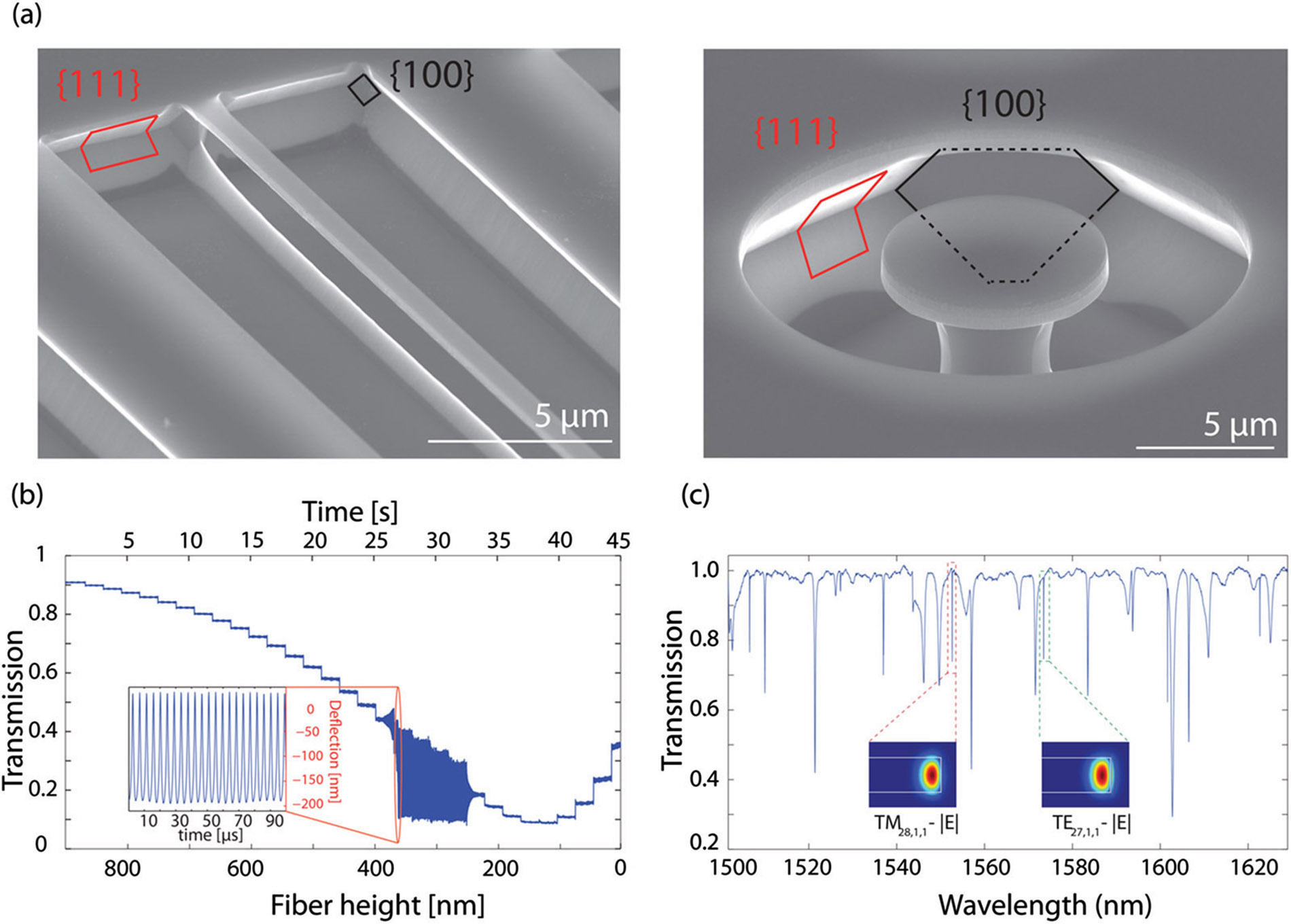
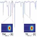
Figure 2. Analysis of fabricated nanobeam and microdisk devices, adapted from original figures. 8, 9 (a) Nanobeam (left) and whispering gallery mode microdisk resonator (right) fabricated from single-crystal diamond. The chemical nature of the undercut is evident from the definition of the {111}and {100}families of crystal planes. (b) Time series data for the output power of the fiber taper for different separation gaps. A high-speed photodetector reveals self-oscillations in the nanobeam (with oscillation amplitudes of more than 200nm). (c) Wavelength-dependent fiber taper transmission profile of a microdisk (with a diameter of about 8μm). Finite difference time domain simulations of the total electric field (E) for the transverse-magnetic-like (TM) and transverse-electric-like (TE) field profiles are shown as insets. The subscripts indicate the azimuthal, radial, and vertical order of the mode, respectively.
To study the optical and mechanical properties of these nanostructures, we use a dimpled tapered optical fiber (with a diameter of about 1μm) to evanescently couple light to and from the device.10 By monitoring the time- and wavelength-dependent transmission through the fiber taper, we can investigate the mechanical and optical characteristics of our fabricated devices. We first fabricated nanobeam structures, such as the device shown in Figure 2(a), using our etching process. These devices have a nominal width and thickness of 500 and 250nm, respectively.9 We chose the cross section for this device so that it has the same effective refractive index as the fiber taper, and thus satisfies the phase-matching condition for nanobeam-fiber taper waveguide coupling. Motion of this nanobeam modulates the transmitted power in the fiber taper when the gap between them is less than 1μm. We monitor this modulation with the use of a high-speed photodetector. We are also able to model this modulation as 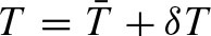 , where , where  is the average transmitted power in the fiber taper. increases with decreasing gap size for gaps of less than 200nm: see Figure 2(b). This reveals the coherent nature of coupling between the nanobeam and fiber taper, and is related to the light that is coupled from the fiber into the nanobeam and back out into the fiber. δT describes the time-dependent fluctuations in the transmitted power, from which the mechanical characteristics of the nanobeam can be examined in frequency space, via a Fourier transform. Although the waveguide coupling nature of this detection scheme limits the dimensions of nanobeams that can be studied, it allows a highly sensitive readout of their mechanical characteristics over a wide optical bandwidth. This optomechanical coupling method can also be fully integrated by replacing the fiber taper with an on-chip waveguide. is the average transmitted power in the fiber taper. increases with decreasing gap size for gaps of less than 200nm: see Figure 2(b). This reveals the coherent nature of coupling between the nanobeam and fiber taper, and is related to the light that is coupled from the fiber into the nanobeam and back out into the fiber. δT describes the time-dependent fluctuations in the transmitted power, from which the mechanical characteristics of the nanobeam can be examined in frequency space, via a Fourier transform. Although the waveguide coupling nature of this detection scheme limits the dimensions of nanobeams that can be studied, it allows a highly sensitive readout of their mechanical characteristics over a wide optical bandwidth. This optomechanical coupling method can also be fully integrated by replacing the fiber taper with an on-chip waveguide.
Our fabricated nanobeam devices support mechanical modes that vary in frequency (from hundreds of kilohertz to tens of megahertz), with quality factors of more than 700,000 at cryogenic temperatures.9 Combined with strong waveguide coupling, thermally driven vibrations of these nanobeams can be amplified via the photothermal force to a regime where self-oscillation occurs at amplitudes of more than 200nm, as shown in the inset to Figure 2(b). Oscillations at these amplitudes create a potential strain coupling rate of about 0.8MHz to NV ground-state spins. This coupling provides a platform to study spin-phonon-photon interactions.
In addition to our nanobeam devices, we have also used the same fabrication method to produce single-crystal diamond microdisk structures, shown on the right of Figure 2(a).8 A typical wavelength-dependent fiber taper transmission profile for this device is shown in Figure 2(c). In this profile, multiple optical resonances are visible. These devices support whispering gallery mode optical resonances, which confine light inside the microdisk via total internal reflection. This results in a small effective mode volume (V) and a high optical quality factor (Q). Our microdisks support both transverse-electric-like and transverse-magnetic-like optical modes with Q of more than 1.1 × 10⁵ and a simulated V of about 11 (λ/n)3 at a wavelength (λ) of 1.5μm, where n is the refractive index of diamond. These devices represent a first step in the realization of hybrid cavity optomechanical structures in single-crystal diamond.
We have developed a new fabrication technique to create optical and mechanical devices from single-crystal bulk diamond. With the use of this approach, we have demonstrated high-quality mechanical resonators and optical cavities. In our future work we will focus on developing cavity optomechanical devices in single-crystal diamond microdisks. By amplifying the thermal vibrations of microdisk mechanical resonances via the radiation pressure force, it will be possible to create large oscillating strain fields in the device. Ultimately, this will allow us to study photon-phonon-spin interactions in a single-crystal diamond optomechanical cavity.
The authors are grateful for funding support from the National Research Council of Canada, the Canada Foundation for Innovation, the Alberta Innovates – Technology Futures program, as well as the Natural Sciences and Engineering Research Council of Canada.
Behzad Khanaliloo, Matthew Mitchell, David P. Lake, Hamidreza Kaviani, John P. Hadden, Paul Barclay
University of Calgary
Calgary, Canada
Paul Barclay is an assistant professor and the Alberta Innovates Scholar in quantum nanotechnology. He also holds a cross-appointment at the National Institute for Nanotechnology in Edmonton, Canada.
Aaron C. Hryciw
University of Alberta
Edmonton, Canada
Harishankar Jayakumar
City College of New York
New York, NY
References:
2. I. Aharonovich, A. D. Greentree, S. Prawer, Diamond photonics, Nat. Photon. 5, p. 397-405, 2011.
3. A. Barfuss, J. Teissier, E. Neu, A. Nunnenkamp, P. Maletinsky, Strong mechanical driving of a single electron spin, Nat. Phys. 11, p. 820-824, 2015.
4. S. D. Bennett, N. Y. Yao, J. Otterbach, P. Zoller, P. Rabl, M. D. Lukin, Phonon-induced spin-spin interactions in diamond nanostructures: application to spin squeezing, Phys. Rev. Lett. 110, p. 156402, 2013. doi:10.1103/PhysRevLett.110.1564025. I. Wilson-Rae, P. Zoller, A. Imamoǧlu, Laser cooling of a nanomechanical resonator mode to its quantum ground state, Phys. Rev. Lett 92, p. 075507, 2004. doi:10.1103/PhysRevLett.92.0755076. K. V. Kepesidis, S. D. Bennett, S. Portolan, M. D. Lukin, P. Rabl, Phonon cooling and lasing with nitrogen-vacancy centers in diamond, Phys. Rev. B 88, p. 064105, 2013. doi:10.1103/PhysRevB.88.0641057. P. E. Barclay, Optomechanics in single-crystal diamond. Presented at SPIE Photonics West 2016.
8. B. Khanaliloo, M. Mitchell, A. C. Hryciw, P. E. Barclay, High-Q/V monolithic diamond microdisks fabricated with quasi-isotropic etching, Nano Lett. 15, p. 5131-5136, 2015.
9. B. Khanaliloo, H. Jayakumar, A. C. Hryciw, D. P. Lake, H. Kaviani, P. E. Barclay, Single-crystal diamond nanobeam waveguide optomechanics, Phys. Rev. X 5, p. 041051, 2015. doi:10.1103/PhysRevX.5.04105110. C. P. Michael, M. Borselli, T. J. Johnson, C. Chrystala, O. Painter, An optical fiber-taper probe for wafer-scale microphotonic device characterization, Opt. Express 15, p. 4745-4752, 2007.
|
|
|